The Invisible Foundation of the AI Boom: 10 Nanotech Stocks to Buy Now
Inside a factory the size of four football fields in Tainan, Taiwan, the air is cleaner than almost anywhere else on Earth.
Workers move carefully between the machines in what are known as “bunny suits” – white, head-to-toe coverings made from non-shedding polyester.
The suits aren’t to protect the workers. They’re to protect what the workers are making.
This is Fab 18 – one of the most advanced industrial plants on Earth. And it’s run by Taiwan Semiconductor Manufacturing Company, or TSMC, the world’s largest chipmaker.
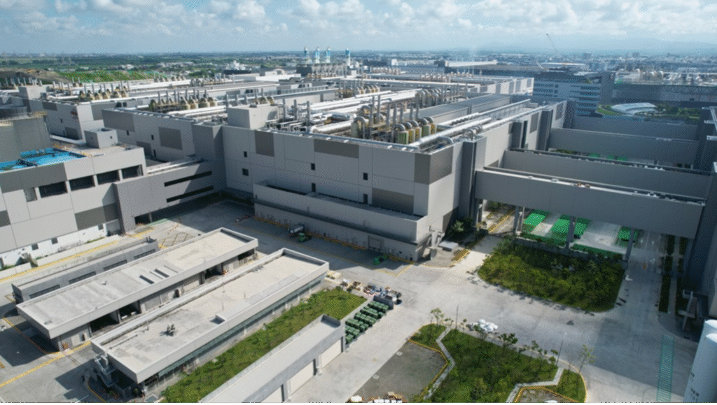
Using beams of light, the machines inside print circuit patterns onto silicon wafers – patterns so small that 10,000 of them laid side by side would barely span the width of a human hair.
At these scales – measured in billionths of a meter – a single out-of-place particle that would be invisible even under a microscope can ruin a chip worth thousands of dollars.
What makes these mind-bendingly small scales possible is nanotechnology: atomic-scale engineering that allows chipmakers to pack billions of transistors onto a silicon wafer the size of your fingernail.
Why does this matter to investors?
Without the ability to build transistors just a few atoms wide – and pack billions of them onto a single chip – today’s AI models couldn’t run.
Consulting giant Deloitte projects the global semiconductor industry will hit $975 billion in sales in 2026, a historic peak fueled almost entirely by AI.
Every dollar of AI spending – every GPU Nvidia sells, every data center Google builds, every model OpenAI trains – depends on machines that can print, deposit, etch, and inspect structures unfathomably tiny.
And the demands are only getting more extreme.
Nvidia’s current Blackwell AI chip contains 208 billion transistors. Its next-generation Rubin chip is expected to pack 336 billion, a 60% increase in a single generation. Each of those transistors is built at the 3-nanometer scale, using the most advanced nanotechnology on Earth.
The ceiling for AI isn’t just software. It isn’t just algorithms. It’s the physics of building at the atomic scale. And the companies that solve those physics problems sit at one of the most critical chokepoints in the entire AI economy.
That makes nanotechnology the invisible foundation beneath the entire AI infrastructure buildout – and one of the most overlooked ways to profit from the AI boom.
So in this report, we’ll look at what nanotechnology is, why it’s critical for the AI revolution, and how to profit from this under-the-radar investment theme.
Forget the Sci-Fi Version of Nanotech
When you hear the word “nanotech,” you may think of the submarine crew shrunk to microscopic size to hunt down disease from inside the human body in the classic 1966 sci-fi movie Fantastic Voyage.

Or you may think of the swarm of self-replicating nanobots that escape a lab and turn predatory in Michael Crichton’s novel Prey.
You may even think of Tony Stark’s nanotech suit in the Marvel movies: billions of tiny particles flowing out of the chest plate to form a full suit of armor in seconds.
In reality, nanotechnology is the science of engineering materials and structures at the scale of nanometers.
A nanometer is one billionth of a meter. To get a sense of that scale, imagine a marble sitting on the ground in front of you. Now imagine the Earth. A nanometer is to a marble what a marble is to the Earth.
It’s what makes it possible to:
- Vaporize tin into 220,000-degree plasma to print circuits a few atoms wide
- Deposit more than 100 films onto a chip, each one measured in tenths of a nanometer
- Build sensors that detect flaws the width of 10 atoms
- Mirrors polished to atomic-level smoothness – if scaled to the size of Germany, the tallest surface bump would be just a tenth of a millimeter
- Purify the chemicals used in chipmaking to standards 50,000 times stricter than drinking water
This isn’t speculative. It’s happening now, at an industrial scale, inside the factories that make the chips in your phone, your car, and the servers behind every ChatGPT, Gemini, and Claude conversation.
Why AI Can’t Advance Without Nanotech
Every AI model – every chatbot, every image generator, every system that drives an autonomous car – runs on chips. And every new generation of AI demands more powerful chips than the last.
But you can’t just make chips bigger. Physics won’t allow it.
More surface area means more heat. And at the speeds AI demands, even a few extra millimeters of distance between transistors creates lag that slows everything down.
The only way to make chips more powerful is to pack more transistors into the same space.
Today’s most advanced chips hold more than 100 billion transistors. That’s more transistors than there are stars in the Milky Way – packed onto a piece of silicon the size of your fingernail.
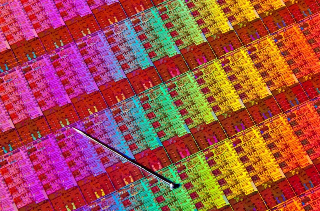
Each one is just a few nanometers wide. That’s the distance of roughly 10 to 20 atoms laid end to end.
Getting to that scale – and manufacturing reliably at it, billions of times over – requires an ecosystem of highly specialized companies. Each one plays a distinct role. Together, they form a supply chain that makes AI possible.
To understand where the profit opportunities lie, it helps to think of this ecosystem in layers – like a building with a foundation, structural beams, walls, and finishes. Each layer depends on the one below it. Miss one, and the whole structure fails.
The Nanotech Stack: Four Layers of Opportunity
The stock recommendations in this report are organized around the roles companies play in the nanotech supply chain. Rather than placing all our chips on one company or one bet, this lets you build exposure across a spectrum – from the large, established names to smaller, more specialized plays.
Here’s how it breaks down:
Layer 1 is the Lithography Layer – the companies that print impossibly small patterns onto silicon. This is where the most extreme physics meets the most advanced engineering on the planet. Without it, nothing else in the stack works.
Layer 2 is the Fabrication Layer — the companies that deposit, etch, and build chips one atomic layer at a time. If lithography is the printing press, fabrication is the ink, the paper, and the binding.
Layer 3 is the Inspection & Materials Layer – the companies that catch defects invisible to any microscope and supply the ultra-pure chemicals and gases that make atomic-scale manufacturing possible. Think of it as quality control at the edge of what’s physically measurable.
Layer 4 is the Compute & Application Layer – the companies that design the chips, build the systems, and deliver the computing power that nanotech makes possible. These are the end users of everything the stack produces – and they sit at the center of the AI boom.
With that framework in mind, here are the companies best positioned to profit as nanotech continues to underpin the AI revolution – and spread into energy, medicine, and beyond.
I. The Lithography Layer
ASML (ASML)
If there’s one company that sits at the foundation of the entire AI supply chain, it’s ASML.
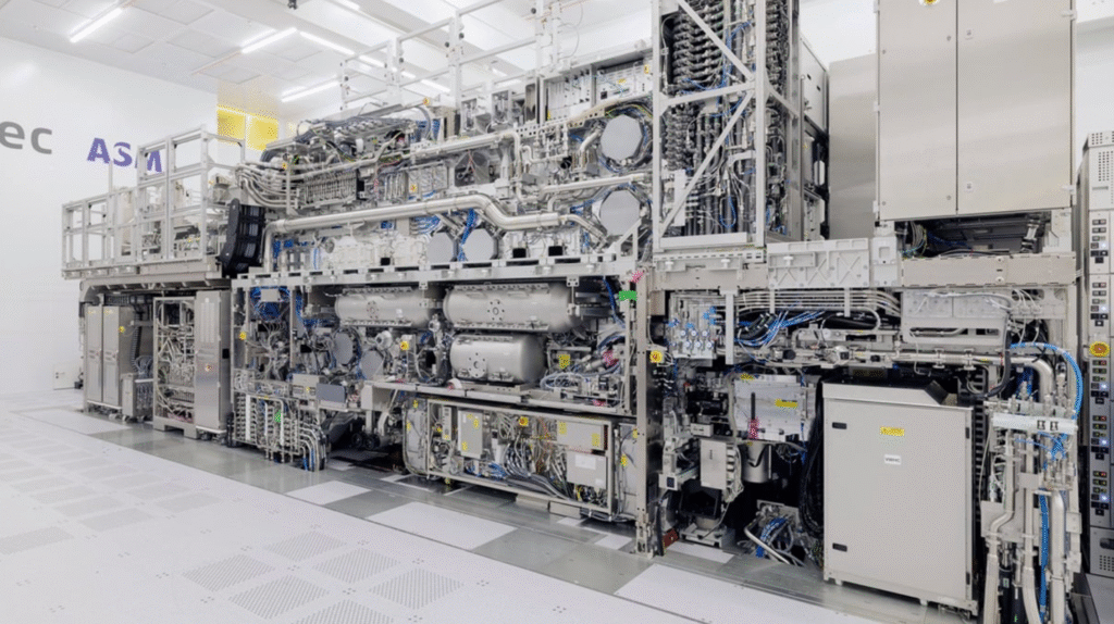
This Dutch company builds the machines that print the nanoscale circuit patterns that make modern chips possible. No other company on Earth can do what ASML does. It holds a complete monopoly on the most advanced chipmaking tool ever created.
Here’s how it works.
Inside each machine, a high-powered laser fires 50,000 times per second at tiny droplets of molten tin. The first pulse flattens each droplet. The second vaporizes it at 220,000°C – roughly 40 times hotter than the surface of the Sun.
The resulting plasma emits a burst of extreme ultraviolet (EUV) light. That light is bounced off mirrors polished so precisely that if you scaled one to the size of Germany, the tallest bump on its surface would be about one-tenth of a millimeter.
The light etches circuit patterns onto silicon. The patterns are so small they can’t be seen with any optical instrument. They exist at the scale of individual atoms.
Each machine weighs as much as two Boeing 737s, ships in about 250 crates, and takes 250 engineers roughly six months to assemble. There are only a few hundred of them on Earth. Each costs north of $300 million.
And every advanced AI chip in existence was made on one of these machines.
ASML is now shipping its next-generation “High NA” EUV systems, which can print features about 1.7 times smaller and achieve transistor densities nearly three times higher than the current generation.
Intel received its first High NA system in April 2024. Samsung is close behind. These machines cost as much as $400 million each.
ASML has guided to 2026 revenue of $34 billion to $39 billion. Its EUV business alone is expected to grow by about 30% this year. And beyond High NA, ASML is already developing “Hyper NA” tools – the next generation after next – targeted for around 2030.
For investors, ASML is as close to an infrastructure monopoly as you’ll find in technology. Every road in the AI economy runs through its machines.
II. The Fabrication Layer
Applied Materials (AMAT)
Once ASML’s machines print a pattern onto silicon, the real construction begins – and Applied Materials is at the center of it.
Think of a chip as a skyscraper built from the ground up, one atomic floor at a time. Each floor is a thin film – some conduct electricity, forming the wiring that connects billions of transistors. Others insulate, stopping signals from crossing and rendering the chip useless.
Applied Materials builds the machines that deposit these films. Inside a vacuum chamber, gases are broken apart and reassembled on the wafer’s surface, building up layers just a few atoms thick.
A single chip can require more than 100 of these layers. Each one is deposited with a precision measured in angstroms – tenths of a nanometer.
At these scales, even a single misplaced atom can cause a chip to fail. Applied Materials’ equipment has to be right every time, across billions of transistors on every wafer.
The company generated more than $28 billion in revenue in its most recent fiscal year. It’s among the largest semiconductor equipment makers by revenue and serves every major chipmaker on the planet, from TSMC to Samsung to Intel.
As chips grow more complex – stacking layers vertically, integrating new materials, and pushing transistor widths to the edge of what’s physically possible – the machines that build those layers become more essential, not less. That’s Applied Materials’ tailwind.
Lam Research (LRCX)
If Applied Materials deposits the layers, Lam Research carves them into shape.
After each thin film is deposited, specific portions need to be removed – precisely, cleanly, and without damaging the layers underneath. This is etching, and it’s one of the most technically demanding steps in chipmaking.
Lam’s machines use chemically reactive gases to strip away unwanted material at the atomic level. The process has to be accurate to within fractions of a nanometer. Remove too much, and you’ve destroyed the circuit. Remove too little, and the transistor won’t work.
As chips move to three-dimensional designs – stacking transistors vertically to fit more computing power into the same footprint – etching becomes even more critical. The deeper and more complex the structures, the harder it is to carve cleanly.
Lam Research generated roughly $18.4 billion in revenue last year and holds a leading market share in its core etch and deposition segments. It’s a direct beneficiary of every increase in chip complexity – and AI is driving the biggest leap in chip complexity in decades.
III. The Inspection & Materials Layer
KLA Corporation (KLAC)
After a wafer is printed and fabricated, it has to be checked for flaws.
The problem is that the defects that matter at these scales are invisible to even the most powerful microscopes.
So chipmakers use electron beams instead. KLA’s systems fire a stream of electrons at a finished wafer and measure the scatter. Using this method, they can detect defects as small as 1 to 3 nanometers – the width of about 10 atoms.
A single advanced wafer can be worth tens of thousands of dollars. A hidden defect – one that slips past inspection – can turn a functional chip into scrap. At scale, that adds up to billions of dollars in lost production.
KLA is the dominant player in semiconductor inspection and metrology. It generated roughly $12 billion in revenue last year. And its role only grows as features shrink. The smaller the transistor, the harder it is to inspect, and the more valuable inspection becomes.
Without nanotech-scale quality control tools, the chips that power AI models and autonomous vehicles would roll off the line with hidden flaws no human eye could ever catch.
Entegris (ENTG)
Every layer deposited on a chip, every gas used in etching, every chemical used in cleaning – all of it has to be extraordinarily pure.
A single contaminating particle – something you’d never notice in any other industrial context – can destroy a chip at the nanometer scale. That’s the challenge Entegris solves.
The company supplies the ultra-pure chemicals, gases, and filtration systems that chipmakers depend on. Its products sit at the intersection of chemistry and precision engineering. They filter out particles smaller than a virus from the materials that touch every wafer.
Entegris also makes the containers that transport wafers between process steps inside a fab. Even at this level, contamination is a risk. The company’s products touch nearly every stage of the chipmaking process.
Revenue has grown steadily as advanced nodes demand ever-higher purity standards. As chipmakers push to 2-nanometer processes and beyond, the materials become more exotic and the purity requirements more extreme. And Entegris is one of the few companies that can meet those specifications.
Bruker (BRKR)
You can’t engineer at the atomic scale if you can’t see at the atomic scale.
Bruker builds the instruments that allow scientists and engineers to visualize, measure, and analyze materials at the level of individual atoms. Its tools include atomic force microscopes, electron microscopes, X-ray analyzers, and spectroscopy systems.
They’re the eyes of the nanotech industry – used in semiconductor R&D labs, pharmaceutical companies, battery research centers, and university labs around the world.
When a chipmaker is developing a new 2-nanometer process, Bruker’s instruments confirm whether the atoms are positioned exactly where they’re supposed to be. When a drug company is engineering a nanoparticle for targeted cancer therapy, Bruker’s tools verify the particle size and surface chemistry.
The company generated more than $3 billion in revenue last year. It’s not a household name – but it’s one of the few companies that provides the measurement tools without which nanoscale manufacturing wouldn’t be possible.
IV. The Compute & Application Layer
Taiwan Semiconductor Manufacturing Company (TSM)
TSMC doesn’t design chips. It builds them – for nearly every major technology company on Earth.
Apple, Nvidia, and AMD – all of them rely on TSMC to turn their chip designs into physical silicon. The company manufactures more than 90% of the world’s most advanced chips, the ones built at the bleeding edge of nanometer-scale engineering.
TSMC’s newest factories produce chips at the 3-nanometer node, with 2-nanometer production expected to start this year. At these scales, a single transistor is so small that quantum effects – the behavior of individual electrons – start to influence how the chip works.
Building reliably at this scale requires mastering every layer of the nanotech stack. TSMC operates the EUV machines, runs the deposition and etch tools, enforces the purity standards, and passes the inspection checks — all at volumes measured in millions of wafers per year.
The company’s revenue hit roughly $91 billion last year. Its capital expenditures – the money it spends building new fabs and buying new equipment – exceeded $40 billion. That spending flows directly to the equipment and materials companies listed above.
For investors, TSMC is the nexus of the nanotech supply chain. Nearly every dollar spent on AI chips passes through its fabs.
Nvidia (NVDA)
If TSMC is the factory, Nvidia is its single most important customer.
Nvidia designs the graphics processing units (GPUs) that power modern AI. Its chips can perform trillions of calculations per second – exactly what’s needed to train and run the neural networks behind AI models like ChatGPT, Gemini, Claude, and the systems driving autonomous vehicles.
These chips are among the most complex objects humans manufacture. Nvidia’s latest data-center GPUs contain more than 200 billion transistors, each just a few nanometers wide. They exist only because the nanotech supply chain – ASML’s lithography, Applied Materials’ deposition, KLA’s inspection – can reliably build at that scale.
Nvidia generated more than $130 billion in revenue in its most recent fiscal year, a figure that has more than doubled in two years. That growth is driven almost entirely by AI demand.
For investors, Nvidia is the clearest expression of why nanotech matters. Without atomic-scale engineering, Nvidia’s chips wouldn’t exist – and without those chips, the AI boom wouldn’t happen.
Broadcom (AVGO)
Broadcom doesn’t get the headlines Nvidia does. But it plays an equally critical role in the infrastructure that AI depends on.
The company designs the networking and connectivity chips that move data between servers, switches, and storage systems inside data centers. AI doesn’t just require fast processors. It requires massive amounts of data moving at high speeds between thousands of machines working in parallel.
Broadcom’s chips handle that traffic. Its products are part of the networking infrastructure of every major cloud provider.
The company also designs custom AI accelerators for hyperscale customers – the handful of tech giants, like Amazon, Google, and Microsoft, that operate data centers at massive scale.
These are chips tailored to specific AI workloads, manufactured by TSMC at advanced nodes, using the same nanotech stack as Nvidia’s GPUs.
Broadcom generated roughly $64 billion in revenue last year. Its AI-related revenue has been growing rapidly as data-center buildouts accelerate. Like Nvidia, it sits at the top of the nanotech stack – benefiting from every advance in atomic-scale manufacturing that makes faster, denser chips possible.
Beyond Chips: Where Nanotech Goes Next
So far, we’ve focused on nanotech’s role in the semiconductor supply chain – and for good reason. That’s where the money is right now.
But the same atomic-scale engineering that powers AI chips is spreading into other industries. These applications are earlier-stage and are edging closer to the kind of atom-scale engineering that once existed only in science fiction. But their trajectories are worth watching.
- Medicine: Drug companies are engineering nanoparticles small enough to cross cell membranes and deliver medicine directly to tumors – sparing healthy tissue from the damage of traditional chemotherapy. Nanoscale biosensors are also being developed to detect cancer biomarkers at concentrations too low for conventional tests. More than two dozen nano-enabled drugs have already been approved by the FDA, with many more in the pipeline.
- Energy: Researchers are using nanomaterials to redesign battery electrodes, increasing surface area by orders of magnitude. That translates into batteries that charge faster, last longer, and store more energy. The same principles apply to solar cells, where nanoscale coatings can capture more light and convert it more efficiently. Nanotechnology in energy applications is a market projected to reach roughly $19 billion by 2028.
- Materials: Nanocoatings – ultra-thin surface treatments engineered at the molecular level – are being applied to everything from aircraft components to smartphone screens. They can make surfaces harder, more resistant to corrosion, and self-cleaning. This market alone is projected to reach $37 million by 2030.
These applications may seem like they’re out of the pages of a sci-fi novel. But they’re extensions of the same engineering already running at scale inside semiconductor fabs. The tools, techniques, and talent are the same. The applications are just spreading outward.
A Word on Risk
To help you match position sizing to the level of uncertainty, here’s how the recommendations in this report break down.
Large-Cap Companies (Lower Volatility, Suitable for Broad Exposure)
- ASML (ASML)
- Taiwan Semiconductor (TSM)
- Nvidia (NVDA)
- Broadcom (AVGO)
- Applied Materials (AMAT)
- Lam Research (LRCX)
- KLA Corporation (KLAC)
These are large, diversified businesses with established revenue streams. None of them require nanotech to be a recognized investment theme to work as investments. Their exposure is real, but it sits alongside many other revenue drivers. For most investors – especially those new to thematic investing – these are the lowest-risk way to gain exposure.
Mid-Cap Companies (More Direct Exposure, More Volatility)
- Entegris (ENTG)
- Bruker (BRKR)
These companies are more tightly focused on the tools, materials, and measurement systems that make nanoscale manufacturing possible. That gives them more direct leverage to the nanotech theme. But it also means their stocks can swing more sharply based on capital spending cycles, individual contract wins, or shifts in chip demand.
Practical Risk Management
A few principles can help when investing in emerging themes like this one:
- Start with the large caps. They provide exposure without requiring the theme to play out perfectly.
- Size small with the mid-caps. More focused companies should represent smaller positions, not your core holdings.
- Expect volatility – and don’t overreact to it. Sharp price moves are normal in technology sectors. Volatility is the price of admission for the chance at outsized gains.
And remember, you don’t need to own everything on the watchlist. This report is a menu, not a checklist. Even one or two well-chosen positions can provide meaningful exposure to the nanotech theme.
Nanotech is not a short-term trade. It’s a long-term structural trend – one that underpins AI, energy, medicine, and advanced manufacturing simultaneously. Matching your position sizes to your time horizon and risk tolerance is just as important as picking the right companies.
From Atom-Scale Engineering to AI-Powered Returns
The AI revolution isn’t just changing how the world works. It’s also changing how we invest.
At TradeSmith, we’ve built our own AI system – not for engineering chips, but for predicting short-term stock moves.
We call it Predictive Alpha.
It’s a large-scale AI model trained on vast amounts of stock market data. And it uses proprietary machine-learning models to forecast the expected price path of thousands of stocks for every trading day over the next month.
We’ve engineered Predictive Alpha using more than 120 million data points. These include…
- 4.2 million historical price outcomes, spanning seven years and more than 2,300 stocks
- 88.9 million daily forecasts, covering 21 forecast days for every stock on each trading day of the year
- Plus, tens of millions of additional “validation runs,” including target-accuracy, pattern recognition layers, and more
Based on this data, Predictive Alpha learns from the past, adapts to the present, and projects the future.
We’ve found that every stock has a specific “profit window” – periods when it has historically made its largest short-term moves. For example, Tesla may have a six-day window, while Apple may have a 15-day window.
Every day, our system finds the ideal window to trade a particular stock.
Predictive Alpha can’t predict the future with 100% accuracy. And it won’t get every trade right. But it can forecast, with up to 85% probability, where stocks will be tomorrow.
And the longer it runs, the smarter it gets. Here are the top 10 wins that it has identified so far…
- 9.5% on SOFI in 3 days
- 9.6% on SOFI in 8 days
- 10.3% on UPST in 1 day
- 11.4% on MCW in 3 days
- 11.6% on ANF in 3 days
- 12.0% on ACCO in 26 days
- 12.6% on SLV in 4 days
- 16.4% on APLD in 6 days
- 17.6% on NTAP in 21 days
- 25.5% on CVNA in 2 days
These aren’t annual returns. They’re happening over a matter of days. Repeating these types of gains over these timeframes is like having a “house edge” on a casino-hopping Las Vegas trip.
Put the “House Edge” on Your Side
Each year, the Nevada Gaming Control Board (NGCB) writes a report on the success of the casinos on the Las Vegas Strip.
We all know the house always wins—this report tells us by how much.
In 2019, tens of millions of people flocked to Las Vegas to play casino games like blackjack, poker, and roulette. The NGCB shows that, collectively, those folks went home $6.6 billion poorer.
The house edge is the percentage of a player’s bet that the casino is likely to win. In other words, it’s the statistical advantage a casino holds in any given game.
Casinos don’t win year in and year out because they get lucky. They have a deep knowledge of probabilities. And they use this knowledge to build an edge into every game they operate.
They make small wins thousands of times a day, millions of times a year. And these small edges, applied relentlessly, pile up.
It’s the same principle behind Predictive Alpha. A 9.5% win in three days is impressive. Sustained across a trading year, those kinds of wins really add up.
The secret to making money – whether in Vegas or in markets – is simple: find your edge and apply it over and over. Predictive Alpha gives you that edge.
See Predictive Alpha in Action
With Predictive Alpha, we didn’t chase the impossible dream of predicting the future or being right 100% of the time. We looked for an edge we could take advantage of over and over again.
Billionaire casino operators know how powerful that kind of edge is. The world’s best traders know it as well.
And as I mentioned up top, you can now put this edge to work for you.
So, if you haven’t already, check out a live demo.
You’ll see how our AI analyzes five top stocks and predicts where their share prices could land over the next 21 days. It’s one of the most powerful trading tools ever developed – and you can try it free.
Just follow the link below. It will take you to the page where you can try out the free demo, live on screen.
When you do, you’ll also see how you can use this same AI system to forecast price movements across more than 2,300 stocks we track. From the nanotech companies in this report to every major stock on Wall Street.
The future belongs to those who embrace AI – both as an investment theme and as a trading edge.
Keith Kaplan
CEO, TradeSmith